Rethinking Chip Design with AI That Can “See”
New study shows that AI systems capable of processing images and language can help optimize computer chip design

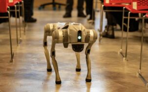
Kempner Graduate Fellow Ikechukwu Uchendu (left) led research to develop VeoPlace, an AI system that helps automate aspects of computer chip design.
Photo: Anna Olivella
At a Glance
- Researchers created an AI system called VeoPlace that can “look at” computer chip layouts and suggest better ways to arrange components.
- The system is designed to support, not replace, engineers by plugging into existing chip design software and suggesting improved chip layouts.
- In tests, VeoPlace produced higher‑quality chip designs than several leading methods, cutting the total distance that signals have to travel between chip components.
Designing the computer chips that power modern electronics has long depended on a combination of mathematical optimization and human visual intuition. Experienced chip designers often rely on spatial reasoning to decide how components should be arranged on a chip — a skill that has proven difficult to replicate with conventional software.
Now, a team of researchers from Harvard and Google DeepMind has developed a chip design system powered by AI software that can “see” and reason about visual chip layouts, improving chip design and potentially benefiting the development of devices ranging from smartphones to AI processors.
The new method, known as VeoPlace (Visual Evolutionary Optimization Placement), uses a Vision-Language Model (VLM) — an AI system trained to process both images and text — to tackle a critical step in chip design known as floorplanning, which involves deciding how electronic components should be arranged on a chip.
“The goal of chip design is to create an arrangement of components such that you get the optimal power, performance, and area metrics,” says Ikechukwu Uchendu, a Kempner Graduate Fellow and the lead author of the study. “So, since Vision-Language Models recently have been shown to do some very complicated vision tasks, we thought: why can’t we use this vision capability to improve automated chip design methods?”
Teaching AI to “see” chip layouts
To build a chip, engineers must arrange components on a virtual “canvas,” deciding exactly where each one should go. The layout affects the quality of the chip, including how fast the chip runs, how much energy it uses, how big it needs to be, and the length of wiring within the chip.
According to Uchendu, a key challenge for fully automating this process has been the sheer number of possible layouts that exist.
“If you have an empty canvas and a number of components that you want to place onto this canvas, using a software program to enumerate and test all the different possible patterns would take you a very long time,” explains Uchendu.
According to Uchendu, even the more limited approach of randomly positioning components and then testing that subset of layouts would still be too time consuming to be practical.
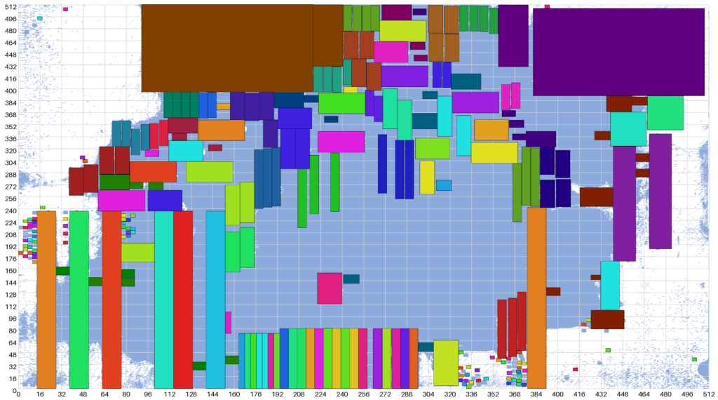
Because it is impractical for chip designers to exhaustively or randomly explore all possible layouts, engineers typically combine automated placement tools with human visual intuition. In practice, designers may manually position major components, define constraints on regions, and use software tools to refine and evaluate the resulting layouts.
Now, VeoPlace offers a different approach. Because VLMs have the ability to emulate human visual intelligence, they can analyze layouts visually and suggest structured arrangements using language, much like a human expert.
“VeoPlace is able to synthesize many prior examples of chip floor plans, and it is able to suggest many new strategies in words,” says Uchendu. “And since its suggestions are in words, they are much more efficient to search than if you were just randomly positioning the components.”
Improving design tools with VeoPlace
Uchendu and his team tested VeoPlace using two types of chip design software: “analytical placer” algorithms, which use mathematical equations to optimize layouts, and reinforcement learning systems, which learn placements through trial and error.
The study compared VeoPlace with several leading approaches to chip design using standard benchmarks — widely used test problems that let researchers compare methods. On nine out of the 10 benchmarks they used, VeoPlace performed better than the leading approaches. It also reduced the total length of wiring — a key metric of chip efficiency — by up to 32 percent. In addition, it improved the performance of the established analytical tools in every tested case, with gains of up to about four percent.
These improvements offer the potential for important real-world impact, says Uchendu. “For the end user, you see benefits from a more efficient chip,” he says. “For example, you could get more battery life on your device, or your device could be smaller.”
Toward AI-assisted chip design
In addition to performance improvements in chip design, VeoPlace demonstrates some distinct advantages of AI systems that can emulate human visual reasoning. In the past, engineers would need to “retrain” AI models with custom data sets for each new task— a process that changes the internal structure of the AI model.
With VeoPlace, the VLM does not need to be retrained. Instead, it generates new, effective layouts by analyzing examples of prior effective layouts. Uchendu says this “training-free” approach is particularly useful in chip design, where relatively little public data is available.
“There’s not much prior knowledge on the internet, because companies don’t release their chip design data,” he says.
He argues that VeoPlace’s ability to perform well without large training datasets points to the reasoning power of VLMs. “They are able to help us with this difficult search problem just from using actual spatial reasoning,” he says.
Looking ahead, the team is working to make VeoPlace faster and able to “look at” even more chip layouts in making design suggestions. Expanding the number of examples the model can use — from dozens to potentially many more — could further improve its recommendations.
Uchendu sees the work as an early step towards more autonomous design tools. “Eventually, we want to have digital assistants for many different problems,” he says. “So I’d say this is the first step towards a digital assistant for chip design.”